
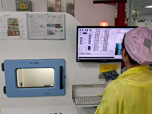
BGA packaging addressed a common issue in electronics assembly: fitting many I/O pins on a component and board with limited space. Instead of moving them around the edges, designers shifted the pins to the bottom, creating rows of solder balls instead of leads. That one move has had a far-reaching effect on PCB assembly, but it also introduced an inspection area that most existing processes simply cannot probe. As BGAs increasingly appear on smartphones, servers and controllers with hundreds or even 500+ I/Os, all of that solder on the underside remains inaccessible.
What Makes BGA Assembly Different From Standard PCB Assembly
In a typical surface-mount process, either an operator or optical inspection (AOI) can directly see all the joints. Solder fillets, lead placement and bridging are all easily visible from this angle. BGA assembly removes that option entirely.
During reflow, the package sits on the board with solder balls compressed between the component and the copper pads. The surface tension of the molten solder does the real work here— it keeps the package aligned and centered as it cools, provided the reflow profile hits the right temperature window. Get the profile wrong, and problems like these show up:
- Head-in-pillow, where the ball and the pad never fully wet together, leaving a joint that looks connected but carries no real mechanical or electrical bond.
- Solder bridging, usually from excess paste volume or a stencil aperture that’s too generous.
- Voiding, gas pockets trapped inside the joint during solidification.
- Cold or cracked joints, often tied to warpage mismatches between the package and the board.
None of these are visible from the outside. That’s the gap X-ray inspection fills.
How X-Ray Inspection Sees What the Eye Can’t
X-ray works by exploiting the fact that solder and board components transmit X-rays at greatly varying rates. Solder alloys are significantly more opaque to X-rays than ceramics, epoxies, silicon, and copper, which make up the rest of the solder joint. That contrast turns an invisible joint into a readable grayscale image—solder shows up bright, and voids and gaps show up dark. An inspector or algorithm can measure exactly what’s going on inside a joint that no camera could ever photograph directly.
2D vs. 3D X-Ray: Which Do You Actually Need?
Most production lines start with 2D X-ray, which is fast and cheap enough to run on a high percentage of boards. It’s genuinely good at catching voids, bridges, and missing balls. It struggles with stacked defects—a void directly behind another void in the same joint can hide because a 2D image flattens everything into one projection.
3D X-ray (often called computed tomography or CT X-ray) solves that by reconstructing the joint layer by layer. Factory data cited in industry BGA inspection guides puts the reduction in false calls from switching to 3D at around 40%, though that comes with a real throughput trade-off. 3D catches more, but it’s slower, so most shops reserve it for high-reliability boards, first-article qualification, or troubleshooting a process that’s already throwing suspicious 2D results.
Another point worth clarifying is that X-ray cannot detect internal package delamination or some crack-type defects, which acoustic microscopy (C-SAM) can readily detect. The “robust” BGA process will therefore usually account for both.
What Counts as a Defect? IPC-A-610 Void Limits
Voiding gets the most attention because it’s the easiest defect to quantify, and the industry has a real number attached to it. Generally speaking, under IPC-A-610, a hole may be acceptable if it’s less than 25% of the surface area of a BGA joint’s solder ball. However, in other regions/groups, there is still a reference to the older Revision G limit of 30%. It may be useful to check which revision the quality system or customer is citing before you set your rejection level.
A few details matter more than the headline number:
- Voids are measured per individual ball, not averaged across the package — a single joint over the limit can fail the whole component even if every other joint looks clean.
- Location matters as much as size. A void sitting right at the pad interface is more damaging to reliability than one centered inside the ball, even at the same area percentage.
- The 25% figure applies across Class 1, 2, and 3 products. What actually changes between classes is inspection coverage — Class 3 work typically moves to 100% X-ray inspection rather than sampling.
Void percentage isn’t just a pass/fail checkbox, either. Consistent voiding above a couple of percent across many joints usually points to an upstream process issue —nitrogen reflow atmosphere, stencil design, or a reflow profile that isn’t fully volatilizing flux—and that’s worth investigating even when every individual joint technically passes.
Building X-Ray Inspection Into the PCB Assembly Workflow
Sliding an X-ray station at the tail-end of the line won’t quite hack it. Inspection will quickly justify itself if it closes the feedback loop back to the process where the error originated.
A workable approach looks something like this:
- Perform 100% 2D X-ray for each BGA and QFN placement as a pass/fail check on the PCB assembly line rather than a spot check.
- Escalate anything borderline — voids near the threshold, irregular ball shapes, suspected bridging — to 3D CT for a definitive call.
- Feed the void and defect data back to the reflow process. If void rates climb, that’s usually a profile or paste problem, not an inspection problem.
- Keep a coplanarity check on incoming BGA components per IPC-7095D; warped packages cause head-in-pillow defects that no amount of downstream inspection will fix retroactively.
That feedback loop is what shops skip when they’re moving fast, and it’s usually the part that reduces defect rates over time rather than just catching them after the fact.
Is X-Ray Inspection Necessary for Every BGA Board?
Not strictly for every board, but it’s close. Anything with a BGA, QFN, or LGA package has hidden joints by definition, so visual and optical inspection can’t verify them. For consumer-grade, low-complexity boards with a mature, well-controlled process, some manufacturers rely on sampled X-ray rather than 100% inspection. For anything going into automotive, medical, aerospace, or other high-reliability applications, 100% X-ray coverage is the standard expectation, and skipping it is a real liability, not just a shortcut.
Getting BGA Assembly Right the First Time
BGA packages aren’t going away—they’re the only practical way to fit hundreds of I/Os onto a shrinking footprint, and the electronics they enable, from smartphones to servers, depend on it. The trade-off is that verifying the result takes more than a trained eye and a good light. X-ray inspection, backed by a defined void standard and a feedback loop into the reflow process, is what turns “the board powered on” into a joint you can actually trust over years of thermal cycling. Any PCB assembly partner working with BGA packages should be able to tell you exactly what void threshold they inspect to and whether that check runs on every board or just a sample—if they can’t answer that clearly, treat it as a red flag.